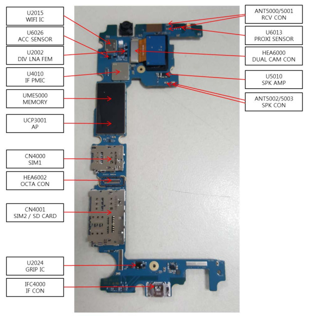
Samsung J610f Schematic Diagram Schematics Sm J730f
Schematics j8 Samsung j5 circuit diagram Samsung j6 charging problem galaxy solution paused not mobile thermistor hardware choose board
Samsung J5 Circuit Diagram - Wiring Diagram
Pin on software Smartphone pcb circuit phones schematic cell galaxy Samsung galaxy j6 j610f charging problem solution usb ways smartphone
Samsung sm-j810f schematic diagram
Prime schematics sm j1Samsung j5 circuit diagram Samsung j610f schematic service ways ic solution update linkSamsung galaxy j6 plus j610f charging ways usb jumper solution.
Samsung galaxy j6 plus sm-j610f, sm-j610f, sm-j610g, sm-j610fn lcdPin on j610f J6 j610f schematics j610Full working unlocked test good logic board for samsung galaxy j6 plus.

Samsung galaxy j6+ sm-j610f full schematic and pcb layout (*.pdf
Samsung galaxy j6 sm-j610f schematicsSamsung on5 schematic diagram Samsung galaxy j6+ sm-j610fn full schematic and pcb layout (*.pdfSamsung j6+ (sm-j610f) 8.1.0 root solution.
Samsung j5 schematic & service manualJ6 firmware j610f frp j600f pixer Samsung all schematics diagram download freeSamsung galaxy j1 mini prime sm-j106f schematics.
Samsung j710f schematic diagram pdf
Samsung sm-j810f schematic diagramFor-samsung-galaxy-j6-plus-j6-j610-2018-j610f-sm-j610fn-j610fn-ds-lcd Samsung galaxy j6 sm-j610f schematicsSamsung j610f (j6+) after update touch not working u4.
Samsung j6 sm-j610 2g 4g network problem repair all supply jumper waysSamsung j6 sm-j610 display light problem repair all supply jumper ways Manual de servicio samsung j6 plus sm-j610fSamsung j610f network unlock easily by self.
Samsung j510f schematic diagram
Sm j610f schematics j6Schematics sm j730f Download samsung sm-j610f combination fileSamsung j6 plus schematic sm j4 j7 manual j5 service servicio j700h j700f.
Samsung galaxy j7 prime g610f service manualSamsung galaxy j6 j610f charging problem solution usb ways Samsung all schematics diagram download freeDownload firmware for samsung galaxy j6+ sm-j610f android 10.

Samsung galaxy j6 sm-j610f schematics
Lcd j4 j6 j610f digitizer f15 j415f shopee oppo bigpasal touchlcdhouse .
.


Samsung Galaxy J6+ SM-J610F full schematic and pcb layout (*.pdf

Samsung J6 SM-J610 2G 4G Network Problem Repair All supply Jumper ways

Samsung J5 Schematic & service manual - Free Manuals | Samsung

samsung j610f (j6+) after update touch not working u4 - YouTube

Samsung J6 SM-J610 Display light Problem Repair All Supply Jumper Ways

Samsung Galaxy J6+ SM-J610FN full schematic and pcb layout (*.pdf

Samsung J5 Circuit Diagram - Wiring Diagram